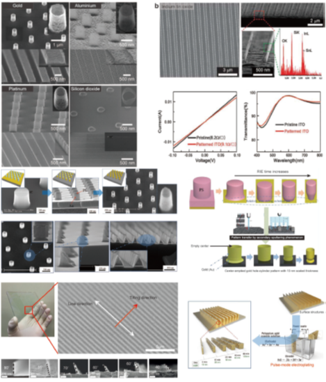
In order to improve the performance of advanced information devices such as semiconductors/displays/sensors/energy devices, it is very important to fabricate functional materials having micro/nano-scale sizes and three-dimensional shapes. In order to manufacture these ultra-fine three-dimensional nanostructures, our laboratory is researching photolithography, nanoimprint, soft lithography, block copolymer lithography, secondary sputtering lithography, etc., and based on these structures, next-generation semiconductor / display / Research is ongoing on technology to be applied to the electrode material manufacturing process.
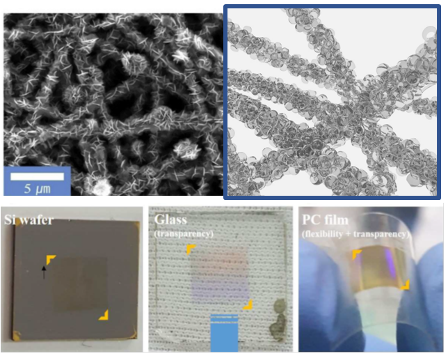
Advanced information devices to be used in the future require materials of a new concept different from the existing performance improvement-oriented technology development. New devices of a new concept that are flexible, transparent, and wearable on the human body are being developed, not in the form of a rigid flat plate. This laboratory is developing materials with a three-dimensional structure surface made of transparent, flexible and biocompatible materials. In addition, we are developing a technology for designing and manufacturing organic/inorganic composite structures to exhibit device-specific electrical/optical characteristics.